1D Model
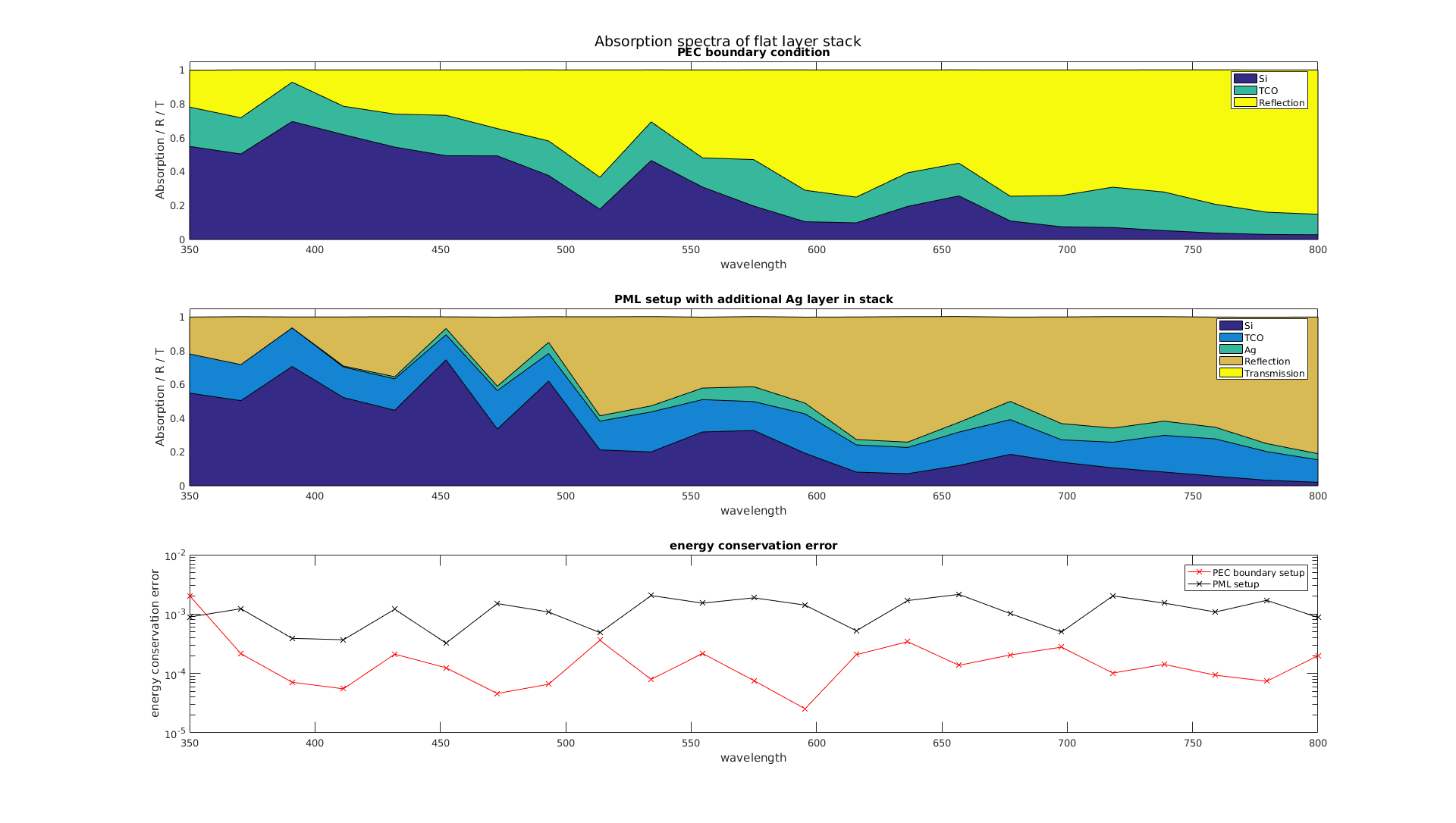
This tutorial example is a one dimensional model of the thin-film solar cell example. It includes a second setup with an additional Ag layer and transparent boundary conditions instead of the perfect electric conductor boundary condition for comparison. The script data_analysis/run_comparison_1D.m performs a wavelength scan for both setups and visualizes the results in an area plot like in the thin-film solar cell example. In addition it shows the energy conservation error in both setups in a semi-logarithmic plot shown at the bottom of Figure 1.
Geometry Definition and Meshing for a 1D system
While source, material and project settings are very similar to the 2D Model, the geometry definition and meshing parameters in the layout.jcm differ slightly.
Layout1D {
  UnitOfLength =1e-9
  Name = "SolarCellLayerStack"
  BoundaryClassLeft = Transparent
  BoundaryClassRight = DomainBoundary
  BoundaryIdRight = 1
  LeftPosition = 0.0
  DomainIds = [1 2 3]
  MaximumSidelengths = [38 21]
  Thicknesses = [600 300 ]
}
In case of a 1D setup the keyword Layout1D is used instead of Layout2D. The file shown above uses the perfect electric conductor boundary condition by assigning a DomainBoundary to the BoundaryClassRight. Further information on the transparent boundary setup and the Layout1D in general can be found in in the Parameter Reference.